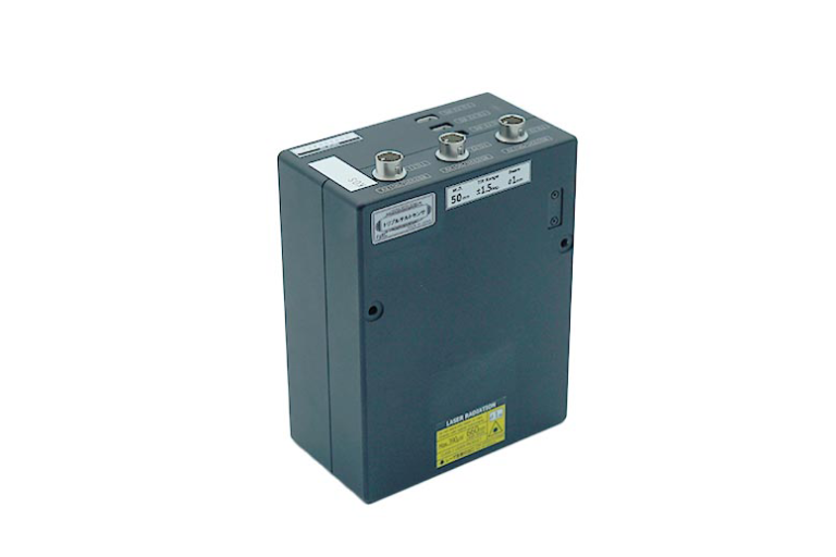
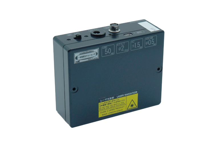
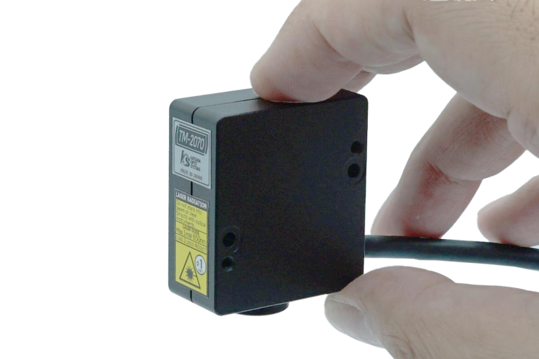
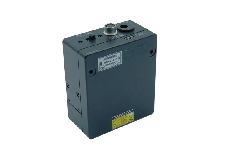
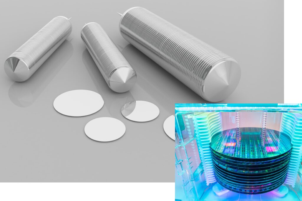
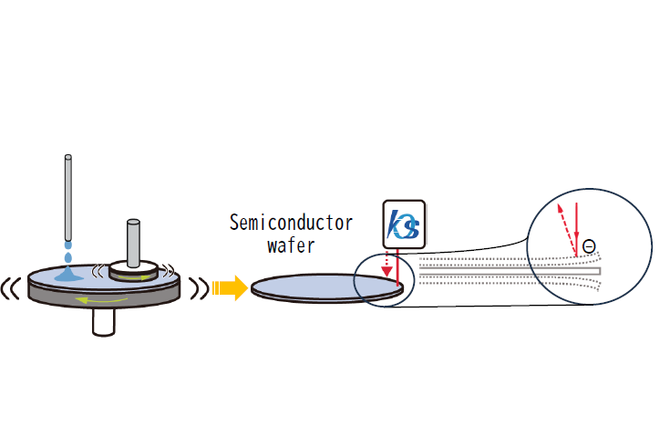
Non-contact measurement of semiconductor wafer shape(warpage) after cutting and polishing
・Issues
After cutting (dicing) and polishing wafers, we want to control the numerical value of warpage.Is there a simple, non-contact method?
・Solutions
Angle measurement of semiconductor wafers after cutting and polishing with a tilt sensor. Numerical control of shape (warpage) is possible without contact. Yield and quality checks become easier.