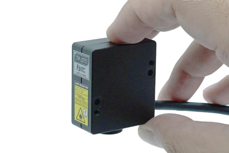
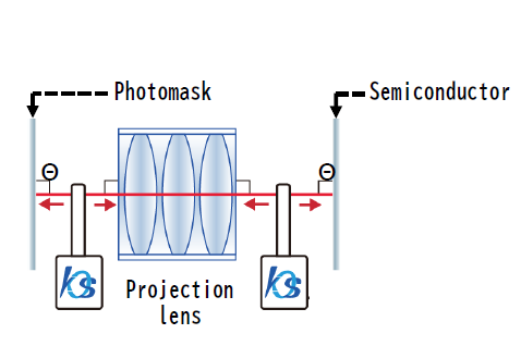
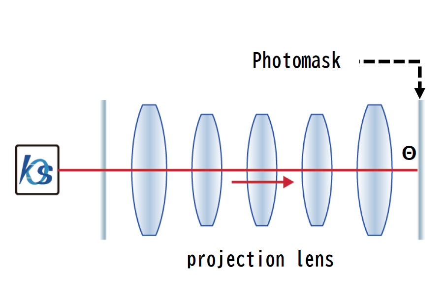
Optical axis adjustment of semiconductor wafer projection (exposure) lens block
・Issues
Is there a way to build projection lens blocks for wafer exposure systems without variation?
・Solutions
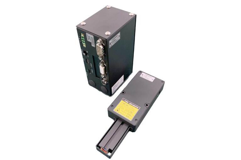
Tilt sensor enables non-contact measurement of the optical axis of the projection lens block, photomask, and lens tilt.This leads to reduced takt time and improved variability.